- 您现在的位置:买卖IC网 > Sheet目录1998 > ICS843156AKILF (IDT, Integrated Device Technology Inc)IC CLK GENERATOR 32VFQFP
ICS843156AKI REVISION B NOVEMBER 28, 2012
17
2012 Integrated Device Technology, Inc.
ICS843156I Data Sheet
CRYSTAL-TO-LVPECL CLOCK SYNTHESIZER
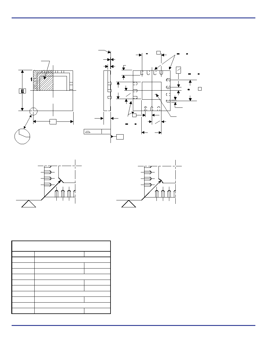
Package Outline and Package Dimensions
Package Outline - K Suffix for 32 Lead VFQFN
Table 9. Package Dimensions
Reference Document: JEDEC Publication 95, MO-220
NOTE: The following package mechanical drawing is a generic
drawing that applies to any pin count VFQFN package. This drawing
is not intended to convey the actual pin count or pin layout of this
device. The pin count and pinout are shown on the front page. The
package dimensions are in Table 9 below.
To p View
Ind exArea
D
Chamfer 4x
0.6 x 0.6 max
OPTIONAL
Anvil
Singula tion
A
0. 08
C
A3
A1
S eating Plan e
E2
2
L
(N
-1)x e
(R ef.)
(Ref.)
N & N
Even
N
e
D2
2
D2
(Ref.)
N & N
Odd
1
2
e
2
(Ty p.)
If N & N
are Even
(N -1)x e
(Re f.)
b
Th er mal
Ba se
N
OR
Anvil
Singulation
N-1
N
CHAMFER
1
2
N-1
1
2
N
RADIUS
4
Bottom View w/Type C ID
Bottom View w/Type A ID
There are 2 methods of indicating pin 1 corner at the back of the VFQFN package are:
1. Type A: Chamfer on the paddle (near pin 1)
2. Type C: Mouse bite on the paddle (near pin 1)
JEDEC Variation: VHHD-2/-4
All Dimensions in Millimeters
Symbol
Minimum
Nominal
Maximum
N
32
A
0.80
1.00
A1
00.05
A3
0.25 Ref.
b
0.18
0.25
0.30
ND & NE
8
D & E
5.00 Basic
D2 & E2
3.0
3.3
e
0.50 Basic
L
0.30
0.40
0.50
发布紧急采购,3分钟左右您将得到回复。
相关PDF资料
ICS843156AKLF
IC CLK GENERATOR 32VFQFP
ICS843202AYILF
IC SYNTHESIZER 680MHZ 32-LQFP
ICS843204AGILF
IC SYNTHESIZER LVPECL 48-TSSOP
ICS84320AY-01LN
IC SYNTHESIZER GP LVPECL 32-LQFP
ICS84320AYI-01LF
IC FREQ SYNTHESIZER 32TQFP
ICS843251AG-04LF
IC CLK GENERATOR LVPECL 8-TSSOP
ICS843251AGI-14LF
IC CLK GEN ETHERNET 25MHZ 8TSSOP
ICS843251BGI-12LF
IC CLK GENERATOR LVPECL 8-TSSOP
相关代理商/技术参数
ICS843156AKILFT
功能描述:IC CLK GENERATOR 32VFQFP RoHS:是 类别:集成电路 (IC) >> 时钟/计时 - 时钟发生器,PLL,频率合成器 系列:HiPerClockS™ 标准包装:1,000 系列:- 类型:时钟/频率合成器,扇出分配 PLL:- 输入:- 输出:- 电路数:- 比率 - 输入:输出:- 差分 - 输入:输出:- 频率 - 最大:- 除法器/乘法器:- 电源电压:- 工作温度:- 安装类型:表面贴装 封装/外壳:56-VFQFN 裸露焊盘 供应商设备封装:56-VFQFP-EP(8x8) 包装:带卷 (TR) 其它名称:844S012AKI-01LFT
ICS843156AKLF
功能描述:IC CLK GENERATOR 32VFQFP RoHS:是 类别:集成电路 (IC) >> 时钟/计时 - 时钟发生器,PLL,频率合成器 系列:HiPerClockS™ 标准包装:1,000 系列:- 类型:时钟/频率合成器,扇出分配 PLL:- 输入:- 输出:- 电路数:- 比率 - 输入:输出:- 差分 - 输入:输出:- 频率 - 最大:- 除法器/乘法器:- 电源电压:- 工作温度:- 安装类型:表面贴装 封装/外壳:56-VFQFN 裸露焊盘 供应商设备封装:56-VFQFP-EP(8x8) 包装:带卷 (TR) 其它名称:844S012AKI-01LFT
ICS843156AKLFT
功能描述:IC CLK GENERATOR 32VFQFP RoHS:是 类别:集成电路 (IC) >> 时钟/计时 - 时钟发生器,PLL,频率合成器 系列:HiPerClockS™ 标准包装:1,000 系列:- 类型:时钟/频率合成器,扇出分配 PLL:- 输入:- 输出:- 电路数:- 比率 - 输入:输出:- 差分 - 输入:输出:- 频率 - 最大:- 除法器/乘法器:- 电源电压:- 工作温度:- 安装类型:表面贴装 封装/外壳:56-VFQFN 裸露焊盘 供应商设备封装:56-VFQFP-EP(8x8) 包装:带卷 (TR) 其它名称:844S012AKI-01LFT
ICS8431AM-21
制造商:ICS 制造商全称:ICS 功能描述:350MHZ, LOW JITTER, CRYSTAL OSCILLATOR-TO-3.3V LVPECL FREQUENCY SYNTHESIZER
ICS8431AM-21LF
功能描述:IC SYNTHESIZER GP LVPECL 28-SOIC RoHS:是 类别:集成电路 (IC) >> 时钟/计时 - 时钟发生器,PLL,频率合成器 系列:HiPerClockS™ 标准包装:1,000 系列:Precision Edge® 类型:时钟/频率合成器 PLL:无 输入:CML,PECL 输出:CML 电路数:1 比率 - 输入:输出:2:1 差分 - 输入:输出:是/是 频率 - 最大:10.7GHz 除法器/乘法器:无/无 电源电压:2.375 V ~ 3.6 V 工作温度:-40°C ~ 85°C 安装类型:表面贴装 封装/外壳:16-VFQFN 裸露焊盘,16-MLF? 供应商设备封装:16-MLF?(3x3) 包装:带卷 (TR) 其它名称:SY58052UMGTRSY58052UMGTR-ND
ICS8431AM-21LFT
功能描述:IC SYNTHESIZER 350MHZ 28-SOIC RoHS:是 类别:集成电路 (IC) >> 时钟/计时 - 时钟发生器,PLL,频率合成器 系列:HiPerClockS™ 标准包装:1,000 系列:- 类型:时钟/频率合成器,扇出分配 PLL:- 输入:- 输出:- 电路数:- 比率 - 输入:输出:- 差分 - 输入:输出:- 频率 - 最大:- 除法器/乘法器:- 电源电压:- 工作温度:- 安装类型:表面贴装 封装/外壳:56-VFQFN 裸露焊盘 供应商设备封装:56-VFQFP-EP(8x8) 包装:带卷 (TR) 其它名称:844S012AKI-01LFT
ICS8431AM-21T
制造商:ICS 制造商全称:ICS 功能描述:350MHZ, LOW JITTER, CRYSTAL OSCILLATOR-TO-3.3V LVPECL FREQUENCY SYNTHESIZER
ICS8431AMI-21
制造商:ICS 制造商全称:ICS 功能描述:350MHZ, LOW JITTER, CRYSTAL OSCILLATOR-TO-3.3V LVPECL FREQUENCY SYNTHESIZER